(China (Mainland))

Product Summary
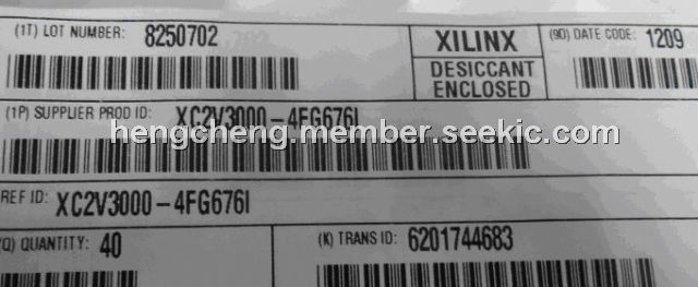
The XC2V3000-4FG676I is a member of the Virtex-II family, which is a platform FPGA developed for high performance from low-density to high-density designs that are based on IP cores and customized modules. The XC2V3000-4FG676I delivers complete solutions for telecommunication, wireless, networking, video, and DSP applications, including PCI, LVDS, and DDR interfaces. The leading-edge 0.15 μm / 0.12 μm CMOS 8-layer metal process and the XC2V3000-4FG676I architecture is optimized for high speed with low power consumption. Combining a wide variety of flexible features and a large range of densities up to 10 million system gates, the Virtex-II family enhances programmable logic design capabilities and is a powerful alternative to mask-programmed gates arrays. The Virtex-II family comprises 11 members, ranging from 40K to 8M system gates.
Parametrics
XC2V3000-4FG676I absolute maximum ratings: (1)VCCINT, Internal supply voltage relative to GND: –0.5 to 1.65 V; (2)VCCAUX, Auxiliary supply voltage relative to GND: –0.5 to 4.0 V; (3)VCCO, Output drivers supply voltage relative to GND: –0.5 to 4.0 V; (4)VBATT, Key memory battery backup supply: –0.5 to 4.0 V; (5)VREF Input reference voltage: –0.5 to VCCO + 0.5 V; (6)VIN, Input voltage relative to GND (user and dedicated I/Os): –0.5 to VCCO + 0.5 V; (7)VTS, Voltage applied to 3-state output (user and dedicated I/Os): –0.5 to 4.0 V; (8)TSTG, Storage temperature (ambient): –65 to +150 ℃; (9)TJ, Maximum junction temperature: +125 ℃.
Features
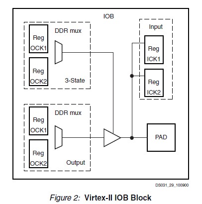
XC2V3000-4FG676I features: (1)Industry First Platform FPGA Solution; (2)IP-Immersion Architecture; (3)SelectRAM Memory Hierarchy; (4)High-Performance Interfaces to External Memory; (5)Arithmetic Functions; (6)Flexible Logic Resources; (7)High-Performance Clock Management Circuitry; (8)Active Interconnect Technology; (9)SelectIO Ultra Technology; (10)Supported by Xilinx Foundation and Alliance Series Development Systems; (11)SRAM-Based In-System Configuration; (12)0.15 μm 8-Layer Metal Process with 0.12 μm High-Speed Transistors; (13)1.5V (VCCINT) Core Power Supply, Dedicated 3.3V VCCAUX Auxiliary and VCCO I/O Power Supplies; (14)IEEE 1149.1 Compatible Boundary-Scan Logic Support; (15)Flip-Chip and Wire-Bond Ball Grid Array (BGA); (16)Packages in Three Standard Fine Pitches (0.80 mm,1.00 mm, and 1.27 mm); (17)Wire-Bond BGA Devices Available in Pb-Free Packaging ; (18)100% Factory Tested.
Diagrams
| Image | Part No | Mfg | Description |  |
Pricing (USD) |
Quantity | ||||||
|---|---|---|---|---|---|---|---|---|---|---|---|---|
 |
 XC2V3000-4FG676I |
|
IC FPGA VIRTEX-II 676FGBGA |
Data Sheet |
|
|
||||||
| Image | Part No | Mfg | Description | |
Pricing (USD) |
Quantity | ||||||
 |
XC2V1000-4FGG256C |
|
IC VIRTEX-II FPGA 1M 256-FBGA |
Data Sheet |
|
|
||||||
|
XC2V1000-4FGG256I |
|
IC FPGA VIRTEX-II 2M 256-FBGA |
Data Sheet |
|
|
||||||
|
XC2V1000-6BGG575C |
|
IC FPGA VIRTEX-II 2M 575-MBGA |
Data Sheet |
|
|
||||||
|
XC2V1000-6FFG896C |
|
IC FPGA VIRTEX-II 2M 896-FBGA |
Data Sheet |
|
|
||||||
|
XC2V1000-6FGG256C |
|
IC FPGA VIRTEX-II 2M 256-FBGA |
Data Sheet |
|
|
||||||
|
XC2V1500-4FFG896C |
|
IC FPGA VIRTEX-II 1.5M 896-FBGA |
Data Sheet |
|
|
||||||